PCI Express Reference Clock Design Considerations (AN45): Difference between revisions
Eugenbeluga (talk | contribs) No edit summary Tag: Reverted |
Eugenbeluga (talk | contribs) No edit summary Tag: Manual revert |
||
| Line 308: | Line 308: | ||
[[Category:Application Notes]] | [[Category:Application Notes]] | ||
Revision as of 03:46, 22 November 2024
| Affected Products | All products |
|---|
Preface
This Application Note provides basic information about the PCIe REFCLK, PCIe reference clock architectures, Spread-Spectrum-Clocking (SSC) feature and provides an example of a typical implementation of a PCIe reference clock buffer.
Terminology
| Term | Description |
|---|---|
| CC | Common REFCLK Rx Architecture |
| CDR | Clock and Data Recovery |
| COM | Computer-On-Module |
| IR | Independent REFCLK |
| PCIe | PCI Express |
| PLL | Phase-Locked Loop |
| REFCLK | Reference Clock |
| SRIS | Separate REFCLK Independent SSC |
| SRNS | Separate Reference Clocks with No SSC |
| SSC | Spread Spectrum Clocking |
Introduction
PCI Express (PCIe) is a high performance, general purpose I/O interconnect defined for a wide variety of computing and communication platforms.
PCIe uses a source-synchronous model. The transmitter supplies the clock to the receiver by embedding the clock into the data stream. A Phase-Locked Loop (PLL) circuit in the receiver recovers the clock.
Additionally, PCIe defines a 100 MHz reference clock (REFCLK) supplied by the system board. This REFCLK is used to derive the local clock that drives the internal logic.
PCIe Reference Clock
The receiver of a PCIe system must generate its own local clock in order to operate its internal logic. The PCIe specification defines different options to generate the recovered clock from the data stream.
Typically, PCIe REFCLK is used to derive the local clock. PCIe REFCLK is specified as a 100 MHz (PCIe 1.0 -PCIe 4.0: +/- 300 ppm, PCIe 5.0 – PCIe 6.0: +/-100 ppm) clock using an HCSL signal logic.
Another important consideration is the jitter performance of the REFCLK. The PCIe specification defines jitter requirements for the different clock architectures and PCIe generations.
The values in Table 1 below are specified by PCI Express® Base Specification Revision 5.0 Version 1.0. The PCIe specification defines that a differential probe must be used to measure REFCLK+ and REFCLK- at the PCIe device with load capacitors CL (Test load CL = 2 pF) and that single ended probes must be used to measure
- VCROSS
- VMAX/MIN
- Rise-Fall Matching
The PCIe specification defines a series of filtering methods that can be applied to the raw REFCLK data. These methods emulate the jitter filtering of the PLL and of the Clock and Data Recovery (CDR), remove low frequency jitter components and minimize measurement-induced jitter.
These filtering methods must be applied to get the effective REFCLK jitter as it appears at the sample latch of the receiver.
There are several tools to characterize the PCIe REFCLK. PCI-SIG and Silicon Labs provide PCIe clock jitter tools. These tools apply the required filtering methods and can be used to characterize the reference clock of all the different PCIe specifications and architectures.
| Min | Max | Unit | |
|---|---|---|---|
| Rising Edge Rate | 0.6 | 4.0 | V/ns |
| Falling Edge Rate | 0.6 | 4.0 | V/ns |
| Differential Input High Voltage (VIH) | +150 | mV | |
| Differential Input Low Voltage (VIL) | -150 | mV | |
| Absolute Crossing Point Voltage (Vcross) | +250 | +550 | mV |
| Variation of VCROSS over all rising clock edges (VCROS DELTA) | +140 | mV | |
| Ring-back Voltage Margin (VRB) | -100 | +100 | mV |
| Time before VRB is allowed (Tstable) | 500 | ps | |
| Average Clock Period Accuracy (TPERIOD AVG) | -300 | +2800 | ppm |
| Average Clock Period Accuracy for devices that support 32.0 GT/s in CC Mode at any speed (TPERIOD AVG_32G_CC) | -100 | +2600 | ppm |
| Average Clock Period Accuracy for devices that support 32.0 GT/s in SRIS Mode at any speed (TPERIOD AVG_32G_SRIS) | -100 | +1600 | ppm |
| Absolute Period (including Jitter and Spread Spectrum modulation, TPERIOD ABS) | 9.847 | 10.203 | ns |
| Absolute Period (including Jitter and Spread Spectrum modulation) for devices that support 32.0 GT/s in CC Mode at any speed (TPERIOD
ABS_32G_CC) |
9.849 | 10.201 | ns |
| Absolute Period (including Jitter and Spread Spectrum modulation) for devices that support 32.0 GT/s in SRIS Mode at any speed (TPERIOD ABS_32G_SRIS) | 9.849 | 10.181 | ns |
| Cycle to Cycle jitter (TCCJITTER) | 150 | ps | |
| Absolute Max input voltage (VMAX) | +1.15 | V | |
| Absolute Min input voltage (VMIN) | -0.3 | V | |
| Duty Cycle | 40 | 60 | % |
| Rising edge rate (REFCLK+) to falling edge rate (REFCLK-) matching (Rise-Fall
Matching) |
20 | % | |
| Refclk Frequency (FREFCLK) | 99.97 | 100.03 | MHz |
| Refclk Frequency for devices that support 32.0 GT/s (FREFCLK_32G) | 99.99 | 100.01 | MHz |
| SSC frequency range (FSSC) | 30 | 33 | kHz |
| SSC deviation (TSSC-FREQ-DEVIATION) | -0.5 | 0.0 | % |
| SSC deviation for devices that support 32.0 GT/s and SRIS when operating in SRIS mode at all speeds (TSSC-FREQ-DEVIATION_32G_SRIS) | -0.3 | 0.0 | % |
| Tx-Rx transport delay (TTRANSPORT-DELAY) | 12 | ns | |
| Max SSC df/dt (TSSC-MAX-FREQ-SLEW) | 1250 | ppm/µs |
Table 1: PCIe REFCLK DC Specifications and AC Timing Requirements
PCIe REFCLK Architectures
Starting with the PCIe Base Specification 2.0, information about the PCIe REFCLK is stated in the electrical section of the specification. This specification introduced three PCIe clock architectures. These PCIe architectures are described in the following sub-sections.
Common REFCLK Rx Architecture (CC)
In the Common REFCLK Rx architecture, both link partners use the same REFCLK as shown in Figure 1 below. This architecture is the most widely supported clocking method.
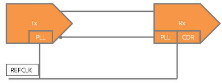
Figure 1: Common REFCLK Rx Architecture
.png)
Note:
Do not directly connect more than one PCIe device to a REFCLK output of the COM. Connect each PCIe device to a unique REFCLK output of the COM or use a PCIe clock buffer. For more information, see section PCIe REFCLK Design Notes
The Common REFCLK Rx architecture improves signal transmission and simplifies the use of SSC because the jitter associated with the reference clock is the same for Tx and Rx.
Additionally, the Common REFCLK Rx architecture improves the behavior in low-power link states as the REFCLK remains available in L0s and L1 link power states. This allows the CDR to maintain the recovered clock even in the absence of the data bit stream.
A disadvantage is that the same clock source must be distributed to every PCIe device. This can be challenging to design for large circuit boards with many PCIe devices.
The PCIe REFCLK contains jitter over a wide range of frequencies. The jitter has an impact on the efficiency of the PCIe data transfer.
The Table 2 below shows the Common REFCLK architecture jitter limits for different data rates. The REFCLK jitter is defined after applying the filtering methods. The jitter at 2.5 GT/s is defined as a peak to peak value whereas the jitter for 5.0, 8.0, 16.0 and 32 GT/s is defined as an RMS value measured from 10 kHz to 50 MHz
| Data Rate | Common REFCLK Jitter Limit |
|---|---|
| 2.5 GT/s | 86 ps (peak to peak) |
| 5.0 GT/s | 3.1 ps RMS |
| 8.0 GT/s | 1.0 ps RMS |
| 16 GT/s | 0.5 ps RMS |
| 32 GT/s | 0.15 ps RMS |
Table 2: Common REFCLK architecture jitter limits
Data Clocked Rx Architecture
In the Data Clocked Rx architecture, the receiver does not use a REFCLK. The receiver recovers the local clock from the transmitter out of the data stream as shown in Figure 2 below.
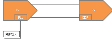
Figure 2: Data Clocked Rx Architecture
.png)
Typically, SSC is not supported in the Data Clocked Rx architecture because the CDR cannot maintain the clock without a common reference.
The Data Clocked Rx architecture is only supported by PCIe 2.0 and 3.0 and is not supported by most chipsets. Therefore, the Data Clocked Rx architecture is usually not recommended.
Independent REFCLK Architecture (IR)
The Independent REFCLK architecture, formerly known as Separate Clock architecture, defines separate reference clocks for Tx and Rx as shown in Figure 3 below.
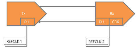
Figure 3: Independent REFCLK Architecture (IR)
.png)
The Independent REFCLK architecture requires very accurate clocks because the variance of the frequency can cause transmission errors.
The PCIe specification does not define jitter limits for the Independent REFCLK architecture. It is up to the designer to implement the REFCLK in order to meet the requirements. However, the PCIe specification defines an Independent REFCLK architecture with no SSC (SRNS) and an Independent REFCLK architecture with independent SSC (SRIS).
Since these architectures use two independent clock sources, the receiver must be able to track and reject the phase drift due to the two independent SSC clocks.
SKP Ordered Sets are used to compensate the differences of the frequencies. The maximum difference with SRNS is 600 ppm which can result in a clock shift once every 1666 clocks. The maximum difference with SRIS is 5600 ppm which can result in a clock shift every 178 clocks.
Overall, it is not possible to guarantee interoperability. Typically, PCIe devices using IR mode cause interoperability issues with a root complex driving data with SSC. Therefore, it is recommended to turn off SSC in IR mode.
Spread Spectrum Clocking (SSC)
Spread Spectrum Clocking (SSC) is a method to modulate the clock frequency in order to improve Electro-Magnetic Interference (EMI) by spreading the signal spectrum around the ideal frequency of the clock.
SSC is not required by the PCIe specification. However, SSC helps a system to pass government emission standards. Typically, the clock can be modulated by 0% to -0.5% (down-spreading) with a modulation rate between 30 kHz and 33 kHz.
SSC is enabled in most x86 based congatec products by default, but can be disabled in the BIOS setup menu. The down-spread modulation can also be adjusted by 0% to -0.5% in the BIOS setup menu.
Note:
SSC is disabled in most ARM based congatec products.
PCIe REFCLK Design Notes
The number of PCIe REFCLK pairs provided by a COM is very limited:
- SMARC - up to three
- COM Express - one
- Qseven - one
In the Common REFCLK Rx architecture, it is not allowed to directly connect more than one PCIe device to a single PCIe REFCLK pair. Therefore, a PCIe clock buffer is often required to distribute the PCIe REFCLK pair from the COM to each PCIe device.
Note:
The REFCLK output of a COM cannot be disabled in most cases. Currently, only the SMARC Specification 2.1 defines PCIe clock request signals for PCIe ports A and B. These signals can be used to disable the respective REFCLK output.
Figure 4 below shows how a PCIe clock buffer can be implemented on the example of conga-TEVAL/COMe 3.0 with an IDT 9DBL0951 clock buffer that provides eight REFCLK outputs.
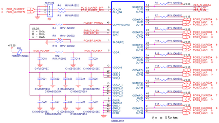
Figure 4: PCIe REFCLK Buffer
.png)
Design Notes:
- The PCIe REFCLK output of the COM must be connected directly to the PCIe clock buffer.
- AC coupling capacitors or external termination resistors are not required.
- The IDT 9DBL0951 PCIe clock buffer in this example provides a direct connection to 85Ω transmission lines. Therefore, no additional termination resistors are required for the REFCLK outputs. Other PCIe clock buffers may require termination resistors. Refer to the datasheet of the respective PCIe clock buffer to check whether termination resistors are required.
- The active low output enable pins (OEx#) are typically connected to the corresponding open-drain CLKREQ# pin of the PCIe device. These pins are used to disable the REFLCK outputs of the clock buffer in low-power link states.
- The IDT 9DBL0951 PCIe clock buffer in this example provides selectable features like slew rate adjustment, differential output amplitude control or impedance adjustment controlled by the SMBus. It is recommended to provide access to these features for further signal adjustment.